
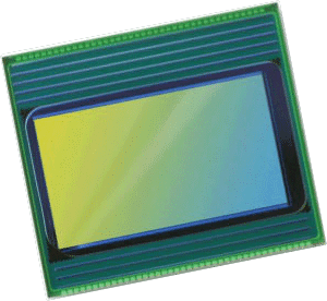
Back-illuminated CMOS Image Sensor
Greater Sensitivity than the Human Eye!
Back-illuminated structure provides higher sensitivity
Sony's back-illuminated CMOS image sensor improves sensitivity and noise reduction - the key factors to enhancing image quality, while radically realigning their fundamental pixel structure from front-illumination to back-illumination. It has retained the advantages of CMOS image sensors such as low power consumption and high-speed operation
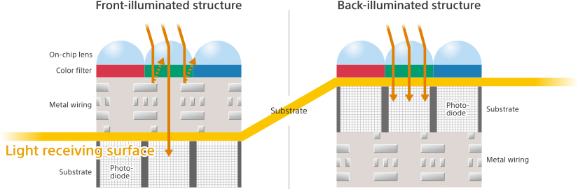
With a conventional front-illumination structure, the metal wiring and transistors on the surface of the silicon substrate that form the sensor's light-sensitive area (photo-diode) impede photon gathering carried out by the on-chip lens, and this has also been an important issue in the miniaturization of pixels and widening optical angle response.
A back-illuminated structure minimizes the degradation of sensitivity to optical angle response, while also increasing the amount of light that enters each pixel due to the lack of obstacles such as metal wiring and transistors that have been moved to the reverse of the silicon substrate.
However, compared to conventional front-illuminated structures, back-illuminated structures commonly causes problems such as noise, dark current, defective pixels and color mixture that lead to image degradation and also cause a decrease in the signal-to-noise ratio.
To overcome this Sony has newly developed a unique photo-diode structure and on-chip lens optimized for back-illuminated structures, that achieves a higher sensitivity and a lower random noise without light by reducing noise, dark current and defect pixels compared to the conventional front-illuminated structure. Additionally, Sony's advanced technologies such as high-precision alignment have addressed any color mixture problems.
CMOS Image Sensor with Column-parallel A/D conversion circuit
Faster than the Human Eye!
|
|
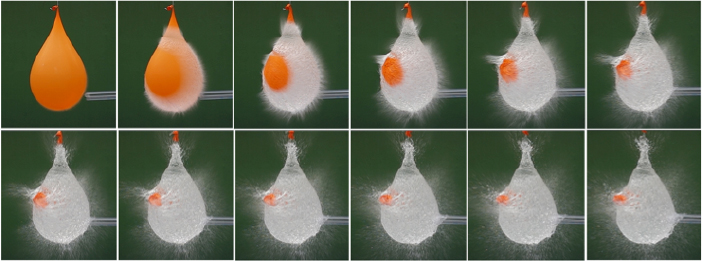
| Een ballon gevuld met water wordt doorprikt. Beeldopname aan hoge snelheid |
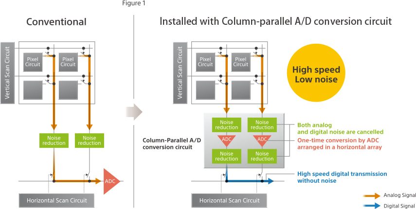
Higher Speed with Column-parallel A/D Conversion and Reducing Noise
The key to increased speed of Sony's CMOS Image Sensor can be found in parallel signal processing. CMOS sensors have analog-digital (A/D) conversion circuits that convert analog pixel signals into digital signals (Figure 1). Speed is increased by arranging thousands of these circuits in a horizontal array and allowing them to operate simultaneously. The A/D conversion circuits used in Sony's CMOS sensors have important characteristics, including the reduced size of the analog circuits in which noise is created, and automatic noise cancellation. This circuit design enables noise reduction to be combined with enhanced speed.
Source : Article and pictures from sony-semicon.co.jp.